In microscopic imaging, two dominant techniques have revolutionized our understanding of the complexity of the nanoworld: scanning electron microscopy (SEM) and transmission electron microscopy (TEM). These powerful tools have opened up new avenues for a variety of scientific disciplines, allowing researchers to delve into the composition, structure, and behavior of a wide range of materials.
We compare and contrast scanning electron microscopy (SEM) and electron microscopy (TEM) by highlighting their respective unique capabilities, applications, and limitations.
1. Scanning Electron Microscopy (SEM):
A scanning electron microscope utilizes an electron beam to scan the surface of a specimen, providing a highly detailed three-dimensional image. The main advantage of SEM is the ability to capture surface morphology from the sub-micron to the nanometer scale with extremely high resolution. By detecting secondary electrons emitted when the beam interacts with the specimen surface, SEM generates topographic images that show surface features, textures, and patterns.
A significant advantage of the SEM is its versatility in elemental analysis using Energy Dispersive X-ray Spectroscopy (EDS). The ability of EDS to identify and map the elements present in a specimen makes the SEM an invaluable tool for materials characterization, forensic analysis, and quality control in a variety of industries.
2. Transmission Electron Microscopy (TEM):
In a TEM, a focused electron beam illuminates a thin section of a specimen, causing electrons to pass through the material. The transmitted electron beam is magnified and focused onto a fluorescent screen or digital camera, producing a high-resolution image of the internal structure of the specimen.
TEM is uniquely suited to study lattice structures, crystal defects, and interfaces between different materials because it provides atomic-level resolution. The ability to examine specimens at such high resolution has led to groundbreaking discoveries in fields such as materials science, nanotechnology and biology. In addition, the TEM can be used for elemental analysis through techniques such as Electron Energy Loss Spectroscopy (EELS) and Selected Area Electron Diffraction (SAED).
3. SEM vs TEM Comparison and Applications:
While both SEM and TEM provide indispensable insight into the microscopic world, they differ in several key ways. Scanning electron microscopes specialize in surface imaging, providing a detailed view of a sample's topography, while TEMs offer higher resolution, revealing a material's internal structure.
Scanning electron microscopy has a wide range of applications, including materials science, geology, archaeology, and biological sciences. It can examine a wide variety of samples such as metals, ceramics, polymers, cells, and tissues, facilitating materials engineering, forensic analysis, and biomedical research.
On the other hand, TEM plays a vital role in the study of nanoparticles, biomolecules, and semiconductor devices. It enables the visualization of atomic structures, the determination of crystallographic orientations, and the study of interfacial properties.TEM plays an important role in the development of nanomaterials, catalysts, and pharmaceuticals, contributing to advances in fields such as nanoelectronics, drug delivery systems, and renewable energy technologies.
4. SEM vs TEM Limitations and Future Developments:
Despite their superior capabilities, SEM and TEM have their limitations. Sample preparation is a critical aspect of both techniques, and TEM requires extremely thin slices of the sample. In addition, both instruments are expensive and require skilled operators to maximize their potential.
Both SEM and TEM techniques have advanced significantly in recent years. Field emission scanning electron microscopy and aberration-corrected TEM have pushed the limits of resolution, allowing researchers to observe finer details. In addition, the development of in situ microscopy techniques has enabled real-time observation of dynamic processes at the nanoscale.
SEM and TEM have revolutionized our ability to explore the microscopic world; SEM excels at surface imaging and elemental analysis, while TEM provides unparalleled atomic-scale resolution and enables the study of internal structure. Together, these technologies continue to drive breakthrough research across disciplines and push our understanding of the nanoworld forward. As technology advances, it is expected that SEM and TEM will be further developed and refined, opening up new avenues for future research and innovation.
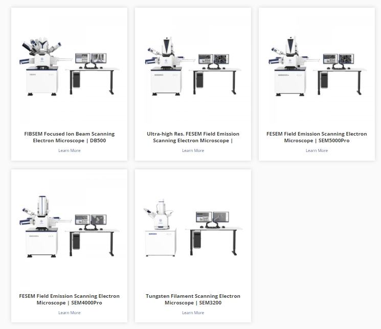
CIQTEK is a manufacturer and global supplier of scanning electron microscopes with leading technology in the industry. They offer a wide range of advanced, well-serviced, and affordable microscopes including FESEM, FIB-SEM, Tungsten Filament SEM, etc. CIQTEK has over 1000+ customers around the world.
>> Website: www.ciqtekglobal.com
>> Email: info@ciqtek.com

